¶ 1 Reference
Digital-Systems-Engineering.pdf
Sam Palermo - ECEN 720: High-Speed Links Circuits and Systems (tamu.edu)
¶ 2 Channel Components
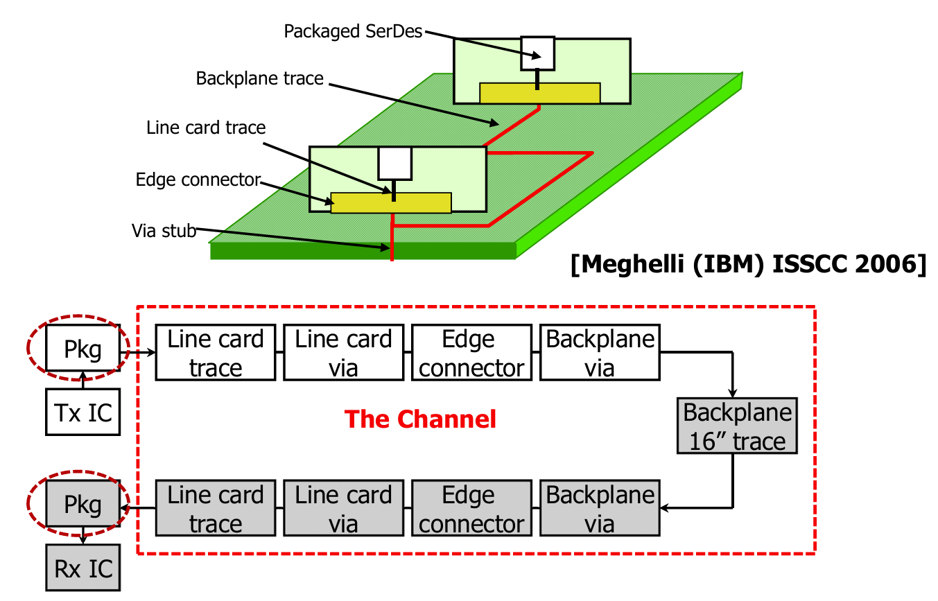
¶ 2.1 IC-Package
¶ 2.2 Printed-Circuit-Boards PCB Stackup
是指印刷电路板(PCB)的堆叠结构或层叠设计。它描述了PCB中的各层之间的排列和构造方式,包括导电层(信号层)和绝缘层(介质层)的排列顺序。
在多层PCB设计中,PCB Stackup 主要包括以下内容:
- 信号层(Signal Layers):用于布置电子元件的信号走线。
- 电源层(Power Planes):专门用于传输电源,如VCC或GND。
- 绝缘层(Dielectric Layers):介于导电层之间,用于绝缘电路并控制信号特性。
¶ 2.3 Connectors
¶ 2.4 VIAs
不同的VIA对信号有不同的影响,表面的Desktop通过信号的能力比较强
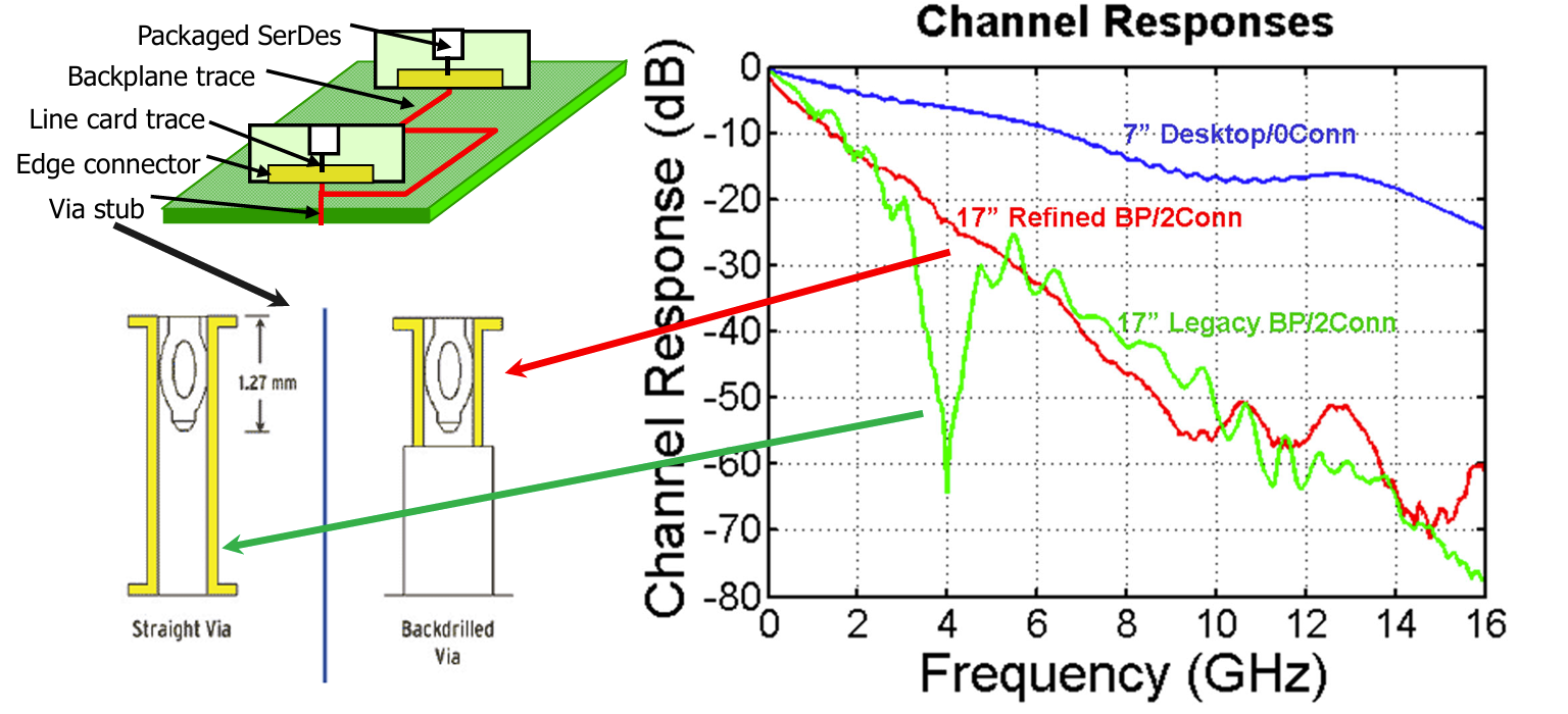
其中Backdrilled via是比较好的,但是成本高贵
- Legacy-Backplane has default straight VIAs: Creates severe nulls which kills signal integrity
- Refined-Backplane has expensive Backdrilled VIAs
[What-is-Back Drilling-in-PCB-Design-and Manufacturing.pdf](/pictures/SerDes/Basics/Modeling-and-Analysis-of-Wires/What-is-Back Drilling-in-PCB-Design-and Manufacturing.pdf)
¶ 2.5 PCB Trace Configurations
- Microstrips are signal traces on PCB outer surfaces: Trace is not enclosed and susceptible to cross-talk
- Striplines are sandwiched between two parallel ground planes: Has increased isolation
¶ 3 Wire Model
¶ 3.1 Resistance
常见的电阻率如下
| Material | Symbol | ρ(Ω·m) |
|---|---|---|
| Silver | Ag | 1.6 × 10⁻⁸ |
| Copper | Cu | 1.7 × 10⁻⁸ |
| Gold | Au | 2.2 × 10⁻⁸ |
| Aluminum | Al | 2.7 × 10⁻⁸ |
| Tungsten | W | 5.5 × 10⁻⁸ |
对于印刷电路板,方块电阻的定义 时,
¶ 3.2 Capacitance
对于带有介质的平行板电容器,电容 的计算公式为:
其中, 是介电常数,单位为法拉每米 (F/m)。
- 包括两个部分:(真空中的介电常数)和 (相对介电常数),即。
- 是电容器极板的面积,单位为平方米 (m²)
- 是极板间的距离,单位为米 (m)
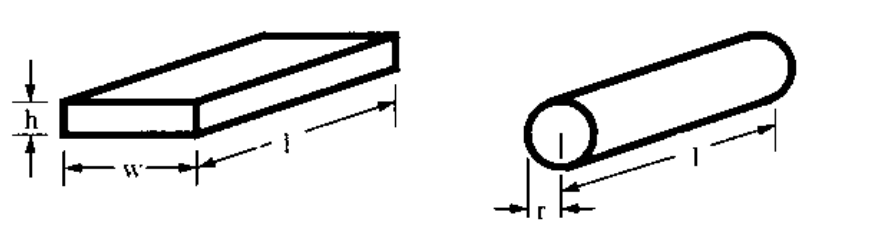
对于不同几何形状 geometry 的走线,其横切面 cross-section 如下,计算单位长度的电容
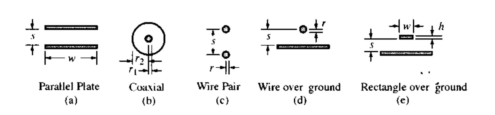
对于宽度 width 远大于间隙 space 的两个 Parallel Plate。首先,我们能够从平行板电容器的横截面计算出单位长度的电容。假设其中一个导体带有电荷密度 Q,我们可以使用高斯定律来求解电场 E。然后,沿着电场线对电场进行积分,就可以确定电压。在最简单的情况下,即平行板电容器中,当板的宽度 w 远大于两板之间的间距时,电场可以被认为是完全被限制在两板之间。在这种情况下,电场是均匀的,其大小为 E=Q/wε。因此单位长度的电容为:
对于 Coaxial, 对于 ,其电场强度为 , 从 到 积分 得到
同轴电缆是一种具有两层同轴结构的电缆:
- 中心导体:电缆的中心部分,通常是铜或铝制,用于传输信号。
- 绝缘层:包裹在中心导体外部,确保信号不会与外层导体直接接触。
- 外导体(屏蔽层):包裹在绝缘层外部,通常是金属编织网或铝箔,用于屏蔽电磁干扰。
- 外绝缘层:包裹在外导体外部,用于保护电缆并隔离外部环境。
同轴电缆广泛用于传输电视信号、互联网连接以及其他高频信号,因其良好的抗干扰能力和信号完整性。
For a parallel pair of wires, we determine the field by superposition, considering just one wire at a time. Each wire gives E=Q/2πx. We then integrate this field from x=r to x=s and combine the two voltages, giving
For single wire over a ground-plane, we apply the principle of charge image; which states that a charge a distance, s, above the plane induces a charge pattern in the plane equivalent to a negative charge an equal distance below the plane. Thus, the capacitance here is equal to twice that of a pair of wires spaced by 2s.
Final geometry, a rectangular conductor over a ground plane, is usually called a microstrip line. Because its width is comparable to its height, we cannot approximate it by a parallel plane, and because it lacks circular symmetry we cannot easily calculate its E field. To handle this difficult geometry we will approximate it by a parallel plate capacitor of width, w, to account for the field under the conductor, in parallel with a wire over a ground plane, to account for the fringing field from the two edges. This approximation is not exact, but it works well in practice.
不同材料的 Permittivity 电介质常数
| Material | εr |
|---|---|
| Air | 1 |
| Teflon | 2 |
| Polyimide | 3 |
| Silicon dioxide | 3.9 |
| Glass-epoxy (PC board) | 4 |
| Alumina | 10 |
| Silicon | 11.7 |
¶ 3.3 Inductance
Whenever the conductors of a transmission line are completely surrounded by a uniform dielectric, the capacitance and inductance are related by
举例,对于情况 (d) 可以得到
对于 ,permeability of free space, \mu_0=4\pi\times10^{-7}\ \text
In situations where there is a dielectric boundary near the transmission line conductors, such as a microstrip line on the surface of a PC board with dielectric below and air above the line, Eq above does not hold. However, it is usually possible to develop approximate formulas for capacitance that define an “average” dielectric constant for these situations, and the inductance can be calculated approximately as shown above.
¶ 4 Transmission Line
¶ 4.1 Partial Equation
传输线是不能集总 lumped 到一个RLC的。传输线可以用偏微分方程描述,而不是差分方程,主要是因为传输线是一个连续的物理系统,而不是离散的系统。在连续系统中,物理量(如电压和电流)可以在任意点定义,并且这些物理量之间的关系可以用连续变化的函数来描述。
使用偏微分方程的底层逻辑在于:
- 连续性:传输线是一个连续的导体,电压和电流在任何位置都可以定义,并且是连续变化的。因此,它们的变化率(导数)可以用来描述系统随时间和空间的变化。
- 局部性:传输线上的物理过程是局部的,即某一位置的电压和电流只与其邻近位置的电压和电流有关。偏微分方程能够捕捉这种局部依赖性。
- 波动性:电磁波在传输线上的传播可以看作是一种波动现象。偏微分方程,特别是波动方程,是描述这种波动现象的数学工具。
- 精确性:偏微分方程提供了对传输线行为的精确描述,可以用来分析传输线的各种特性,如反射、传输损耗、群延时等。
尽管在实际计算中,可能会使用数值方法(如有限差分法)将偏微分方程离散化,从而转换为差分方程来求解,但这并不改变传输线作为一个连续系统的事实。差分方程是偏微分方程的一种数值近似,用于在计算机上求解连续系统的数学模型。
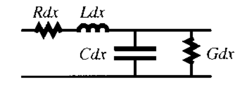
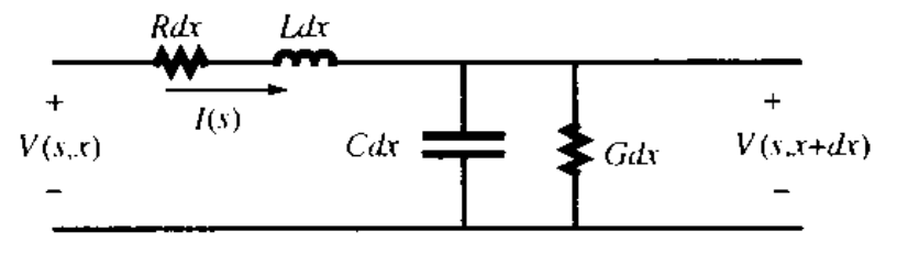
假设在这个节点的电压和电流是 和 ,经过这样一小段传输线后,电压的变化反映到串联的电阻 和电感 上;电流的变化反映到并联(流走了)的电容 和导纳 上,因此可以列出以下方程
上述方程约去 ,然后进一步忽略 ,可以得到
¶ 4.2 Impedance of an Infinite Line
传输线具有恒定阻抗 ,也成为特性阻抗 Character Resistance。因为在传输线上任意的一点,其电压与电流的比值是固定的假设传输线是均匀且无源的,这意味着在其长度上,传输线的物理结构和电磁特性不会发生变化。因此,沿线各点的阻抗保持不变。
对于无限长的传输线,如果认为这个传输线存在阻抗 ,那么在这个传输线上增加 长度后,应该仍然是
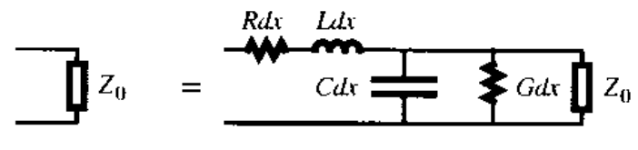
那这样可以列出方程,并进行化简得到
这里,认为 无限小,infinitesimal,这样得到
¶ 4.3 Frequency Domain Solution
将上述的 代入,得到
求解这个微分方程,得到
这里的 是 propagation constant,代表了 per unite distance 下的 magnitude attenuation 和 phase shift
¶ 4.4 Signal Return
再这张图中,上面的 conductive 的 R 和 L 是 signal path,而下面的导线是 return path;如果认为存在流入 signal path,那么必然有一个负向的电流通过 return path 流回。虽然这幅图中的 return path 的阻抗为零,但实际上是存在有限阻抗的;
对于 symmetric twisted-pair cable, return path 的阻抗等于 signal path 的阻抗;
¶ 4.5 Lumped Model of Transmission Lines
在 SPICE 仿真中,可以将多长的 分割出来呢,As a rule of thumb,仿真器的仿真步长(或者说是积分步长)为 ,波形的上升时间为 应该满足以下关系:
亨利(Henry),电感量纲
法拉(Farad),电容量纲
欧姆(Ohms),电组量纲
那么这样就很容得出 和 的量纲是时间,这里在传输线分布参数模型中,和 都是单位长度的 和 ,因此要再乘以
¶ 5 Simple Transmission Line
¶ 5.1 Lumped Capacitive Load
如果信号穿过导线所用的时间相比信号中最快频率成分的上升时间还要小,而且没有DC电流,那么传输线中的 R 和 L 可以放心地忽略。
比如芯片中长度小于 且用于驱动静态栅极的 on-chip wire。这里的 大概率是芯片制造中的特征尺寸,作者说1997年的 technology 是1.2μm);
或者 (这里 是上升时间, 是 propagation velocity)的 off-chip wire 可以堪称是 capacitive load。比如 的 off-chip 长度要小于 6cm。 propagation velocity 和 光速 以及 介电常数 的关系如下
此时更多的问题可能是 cross talk。
¶ 5.2 Lumped Restive Load
对于传输电流且电压相对恒定的电源线,通常会以 Lumped Restive Load 去对待。即使这样的导线上存在很大的电容,但是由于电压恒定不太会有充放电的行为,因此电容还是可以忽略。这样的线重要的考虑是 IR Drop。
¶ 5.3 Lumped Inductive Lines
通常较短且传输较大交流电流的电力传输线(AC power distribution wire)以 Lumped Inductor 去建模
¶ 5.4 Lumped Model of Impendence Discontinuities (不懂)
如果一个LC传输线的 ,这个线中的一部分的阻抗 ,那么这根线可以用 和 串联来建模(这里的 是 length of discontinuity,之所以要乘以长度是因为这里的 LC 通常是以单位长度的 LC 去看的)
同理,对于线中的一部分的阻抗 ,那么这根线可以用 和 串联来建模
¶ 6 RC Tansmmision Line
对于芯片上较长的传输信号的走线,电阻和电容很大,而电感可以忽略。信号传输可以用偏微分方程 #4.1 Partial Equation 来表示
这个表达式是 heat / diffusion equation 热扩散方程,随着走线增加,信号的边沿逐渐消失。因为随着走线延长,R和C都会同时增加,因此信号的延迟RC和长度是平方关系。
¶ 6.1 Step Response of an RC Line
经验参数,对于单位长度下的 ,在长度为 的RC传输线上,延迟时间为
上升时间为
个人理解,这不就是阶跃响应的几个 嘛!
¶ 6.2 Low Frequency RC Lines
对于存在比较大的 L 的传输线,如果频率比较低,这个电感还是可以忽略
典型的应用是电话线,电话线的截止频率频率是33kHz,使用的是AWG24 twisted pair cable,R=0.08Ω/m,C=40pF/m,L=400nH/m,在这个截止频率下信号的实部阻抗为100Ω。在电话线的频率范围300 ~ 3000Hz,阻抗变化1500Ω ~ 500Ω,而 phase shift 一直是 -45°。电话电路的阻抗为600Ω,反应了信号在中频(1KHz)时的阻抗.
在数字系统中,如果使用了长传输线,由于电阻和电容效应,低频分量会导致信号色散(不同频率成分传播速度不同)。信号的高频分量被削弱,导致波形变缓,这种行为被称为低频RC效应。
由于色散行为(Disperse Behavior),信号在接收端发生符号间干扰(ISI),即一个符号的尾部和下一个符号的头部重叠,影响系统的信号完整性,导致误码或信号无法准确恢复。
¶ 7. Lossless LC Transmission Lines
¶ 7.1 Traveling Wave
对于绝大部分 off-chip 传输线,他们不够长不足以集总成电容模型,比较短所以忽略了他们的电阻,因此 #4.1 Partial Equation 忽略了电阻后得到
这样的偏微分方程下,信号的传播是Traveling waves。
Traveling waves 是指沿着传输线以恒定速度传播的波形,它们不会因为传播而变形或失真。这种波的形状保持不变,只是位置随时间推移而变化。
这里 propagation velocity 可以表示为
为了证明这些表达式是微分方程的解,分别求解方程中的 和 \dfrac{\partial^2 V_f(x, t)}
同理,有
这样可以看到,Forumula(7.1.2) 完全吻合Equation(7.1.1)
在这个求证过程中,我们看到traveling waves 满足波动方程,这意味着它们对距离的偏微分和对对时间的偏微分的比值恰好是速度。
¶ 7.2 Impedance and Driving LC Transmission Lines
忽略掉R后,依据#4.2 Impedance of an Infinite Line中求解的公式,可以得到
对于一个电压源,驱动这样的传输线,那么在传输线两端的电压为
两种常用的等效电路分别是戴维宁等效电路(Thevenin equivalent circuit)和诺顿等效电路(Norton equivalent circuit)。前者是电压源+串联电阻,后者是电流源+并联电阻。